Revolutionizing large-scale microstructure analysis
With our Directional Reflectance Microscopy (DRM), crystal orientation mapping at a scale of an XL pizza is no longer impossible!
OUR SOLUTION
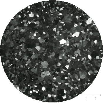
Our DRM technology allows resolving the atomic lattice orientation of crystalline solids through the analysis of their anisotropic surface reflectance. Because DRM is entirely based on optical microscopy, it requires no vacuum and can be employed over large areas. These features enable fast, cost-effective, and previously impossible crystallographic measurements of the entire components.
DATA-DRIVEN APPROACH
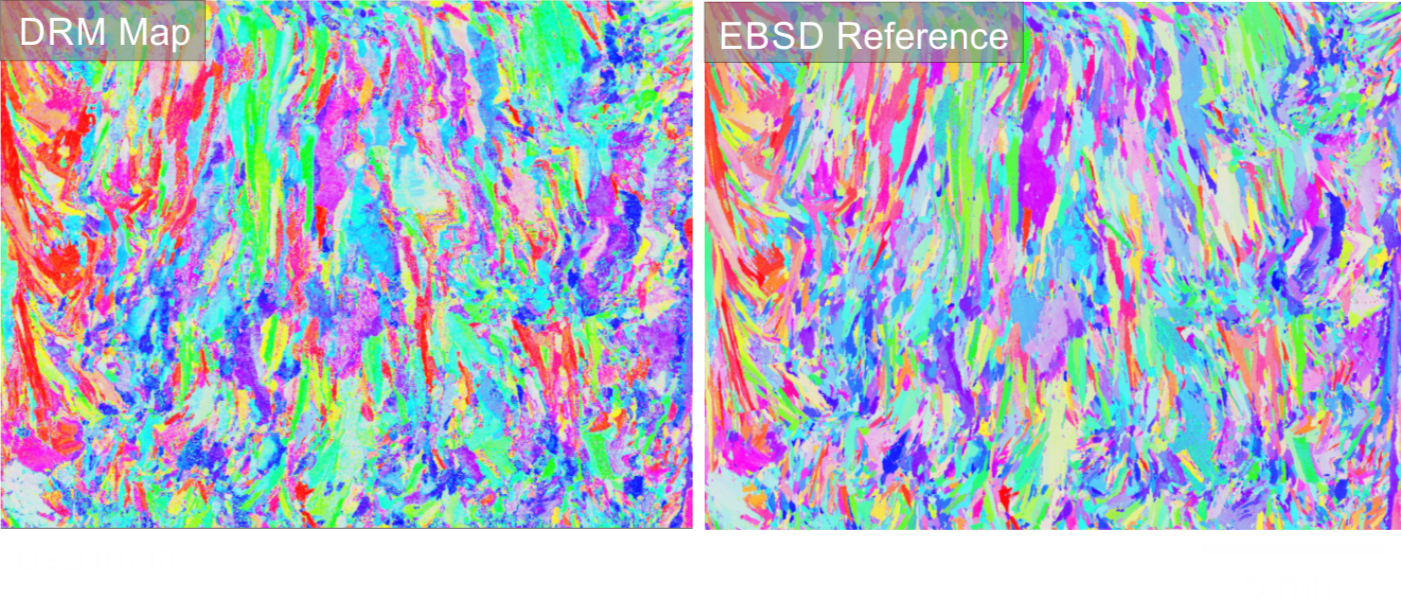
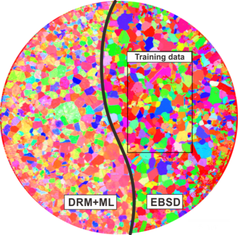
We rely on machine learning models to index crystallographic orientation from the anisotropic surface reflectance signals measured by DRM. After an initial calibration against electron back scatter diffraction, the models provide robust and reliable orientation predictions for a variety of different metal alloys, ceramics, and even composite materials.
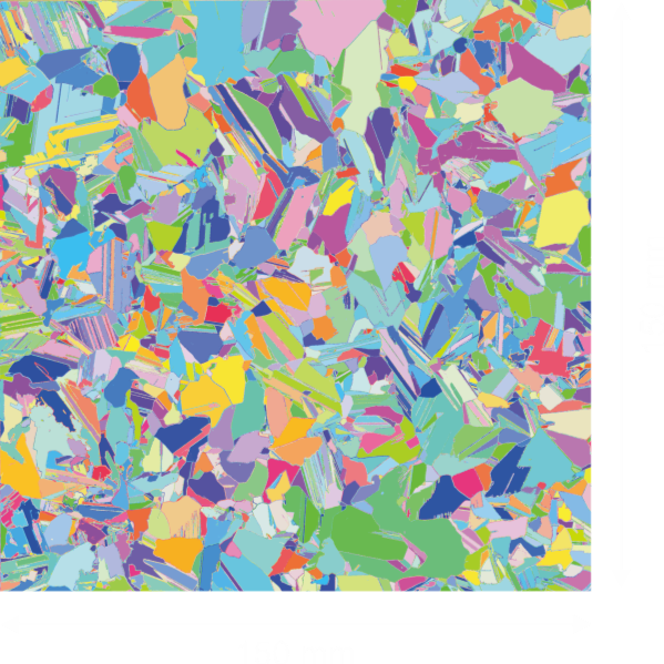
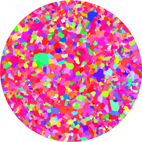
NOT ONLY FOR METALS
The DRM map here was captured from an entire polycrystalline silicon wafer. It would be impossible to take an EBSD scan of such a large sample. DRM could also be used as an in-line characterization technique to inspect batches of entire parts in series.
PRODUCT & SERVICE
Customized DRM Equipment
At XtaLight, we understand that every business has unique needs and requirements when it comes to microstructure characterization. Different materials, different sample size, parts with non-standard geometry, spatial resolution and measurement throughput, investment cost, etc.. Therefore, we offer customized solutions that cater to the specific needs of each customer, including custom-made equipment and software. Our experienced team of engineers and material scientists will work closely with you from the beginning to identify the most suitable solution.

Measurement Services
We also offer a comprehensive range of microstructure analysis services for materials that our current database supports. These measurements include surface analysis and finish quality, grain size and crystallographic orientation mapping, and more. Our services focus on analyzing these quantities over large-size components that are not fit to traditional electron-based characterization methods.
SCIENTIFIC ARTICLES
A machine learning approach to map crystal orientation by optical microscopy
Optical metallography of fusion-based additively manufactured metals
An automated and unbiased grain segmentation method based on directional reflectance microscopy
Measuring crystal orientation from etched surfaces via directional reflectance microscopy
Optical Characterization of Grain Orientation in Crystalline Materials
About Us
Xtalight is a joint venture between Nanyang Technological University (Singapore) and the University of Cambridge (UK). Our team of experts includes materials scientists, mechanical engineers, and data analysts with multi-year experience on materials structure, equipment design, and artificial intelligence. We strive to offer customized solutions for large-scale, high-throughput microstructure characterization, which would otherwise be impossible to achieve using conventional electron-based methods. Talk to us to know more about how DRM technology may help you in your business or your research endeavors!
SUPPORTED BY

© 2025 XtaLight